Protecting Your Technology Investments From Electrostatic Discharge (ESD)

While it may sound like a complex phenomenon, electrostatic discharge is a basic principle of physics.
When matter – for example, a human finger – comes into contact with other things – for example, a membrane switch – the electrons discharge as energy, known as electrostatic discharge.
And while ESD may seem like an occasional nuisance – a tiny shock from a handshake or a few wrinkles on your clothing – ESD discharges into equipment are often a literal shock to the system.
In fact, the ESD Association notes that ESD has been a problem for centuries:
“As early as the 1400s, European and Caribbean military forts were using static control procedures and devices trying to prevent inadvertent electrostatic discharge ignition of gunpowder stores. By the 1860s, paper mills throughout the U.S. employed basic grounding, flame ionization techniques, and steam drums to dissipate static electricity from the paper web as it traveled through the drying process.”
With the modern omnipresence of electronic equipment, ESD is a massive threat. A sudden electrostatic discharge can easily reach up to 15,000 volts and fry delicate electronic equipment in a nanosecond.
“The cost of damaged devices themselves ranges from only a few cents for a simple diode to thousands of dollars for complex integrated circuits,” an ESDA report notes. “When associated costs of repair and rework, shipping, labor, and overhead are included, clearly the opportunities exist for significant improvements.”
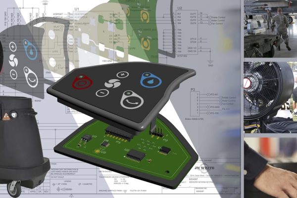
Since membrane switch keypads and custom membrane switches are constantly bombarded with user touch, ESD shielding may need to be deployed as part of the overall design and installation process. At JN White, we create customized ESD shielding solutions based on our customers’ individual needs. ESD shields are generally installed into the user-interface panel under the top-mounted graphic overlay.
How does JN White create the perfect ESD solution?
We generally use two methods – installation of a screen-printed grid pattern of conductive silver ink or the use of full conductive laminates, tapes and foils inside the product.
A grid pattern is usually grounded to a trace on the interface panel which is then routed to a ground plane on the motherboard. This strategy carries the static charge away from any nearby conductive components.
The use of laminates, tapes and foils can deliver a deeper level of dissipative properties. When determining a client’s needs, we consider the absorptive properties of the overlay materials in determining which technique should be used.
Recently, a medical device company came to us in need of a membrane switch solution that would pass an extremely stringent electrostatic discharge (ESD) testing protocol. Specifically, the device would need to withstand a 15kV charge at any given time. In fact, many medical devices require some level of ESD shielding to comply with government and industry standards and regulations.
The Solution
To meet these stringent standards, JN White engineered a unique shielding concept. We began with a three-layer etched copper flex circuit. Next, we sandwiched the sensitive circuitry between two layers of grid shields. By stitching around the perimeter of the three layers, we were able to connect both the top shield and the bottom shield. This grid-shield array then enveloped the electrical components, protecting them from any discharge. In short, we created a next-level Faraday cage to guard all active circuitry. Finally, we added an ESD diode at each LED circuit component of the circuit, protecting the sensitive LEDs inside the ESD cage.
Of course, every ESD need is different. There are a number of factors that will inform your decision, and we’re ready to help you on the journey.
Contact our team to discuss which ESD shielding is right for your membrane switch array.
More from Ken

Manufacturing is evolving—and so are we. As JN White continues to expand our value-added assembly services, we’ve taken an important step forward: investing in additive manufacturing technology with the addition of a new in-house 3D printer. This isn’t just about adding new…

NIST Special Publication (SP) 800-171 is the cybersecurity standard that the Department of Defense (DoD) relies on to protect Controlled Unclassified Information (CUI) in non-federal systems. It defines 110 security requirements across 14 control families, along with 320+ assessment objectives that organizations must meet…
In today’s rapidly evolving technological environment, the need for innovative and dependable membrane switch prototypes is continuously increasing. As a leading membrane switch manufacturer, JN White excels in crafting custom membrane switch prototypes that not only meet your specific design…